ESP32-S3: pin names, applications, and sample projects
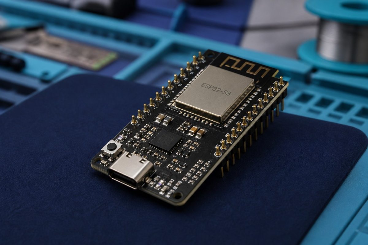
A practical guide to the ESP32-S3 DevKit: header pin names, what each group is for, real applications, and starter projects. Shop boards and parts when you are ready to build.
The ESP32-S3 is Espressif's Wi-Fi and Bluetooth MCU built for products that need more GPIOs, USB, and AI / camera-class peripherals than a classic ESP32. You buy it as a module (WROOM / WROOM-1 / WROOM-2) or as a DevKit with two 22-pin headers.
This post uses the ESP32-S3-DevKitC-1 v1.1 pin names from Espressif. Clone boards print the same silk, but always check your module variant: octal PSRAM boards lock GPIO35, GPIO36, and GPIO37 inside the module. You can edit every section later in Admin - Blog Post.
What the ESP32-S3 is good at
Dual-core Xtensa LX7 up to 240 MHz, Wi-Fi 4, Bluetooth 5 LE, native USB (OTG), more usable GPIO than ESP32, touch pads, ADCs, LCD and camera interfaces, and optional PSRAM for frames or models.
Power the DevKit from USB-C (5 V on the 5V pin) or from a clean 3.3 V rail. Logic is 3.3 V. Do not drive 5 V into a GPIO.
Pin names on the DevKit (J1 left header)
USB at the bottom, antenna at the top. Left header J1, top to bottom:
1. 3V3 - 3.3 V output from the onboard regulator
2. 3V3 - same 3.3 V rail
3. RST - chip enable / reset (EN)
4. 4 - GPIO4, TOUCH4, ADC1_CH3
5. 5 - GPIO5, TOUCH5, ADC1_CH4
6. 6 - GPIO6, TOUCH6, ADC1_CH5
7. 7 - GPIO7, TOUCH7, ADC1_CH6
8. 15 - GPIO15, U0RTS, ADC2_CH4, 32K XTAL_P
9. 16 - GPIO16, U0CTS, ADC2_CH5, 32K XTAL_N
10. 17 - GPIO17, U1TXD, ADC2_CH6
11. 18 - GPIO18, U1RXD, ADC2_CH7
12. 8 - GPIO8, TOUCH8, ADC1_CH7
13. 3 - GPIO3, TOUCH3, ADC1_CH2
14. 46 - GPIO46 (strapping; keep it quiet at boot)
15. 9 - GPIO9, TOUCH9, ADC1_CH8, FSPI HD
16. 10 - GPIO10, TOUCH10, ADC1_CH9, FSPI CS
17. 11 - GPIO11, TOUCH11, ADC2_CH0, FSPI MOSI
18. 12 - GPIO12, TOUCH12, ADC2_CH1, FSPI CLK
19. 13 - GPIO13, TOUCH13, ADC2_CH2, FSPI MISO
20. 14 - GPIO14, TOUCH14, ADC2_CH3, FSPI WP
21. 5V - USB 5 V (when powered from USB)
22. G - Ground
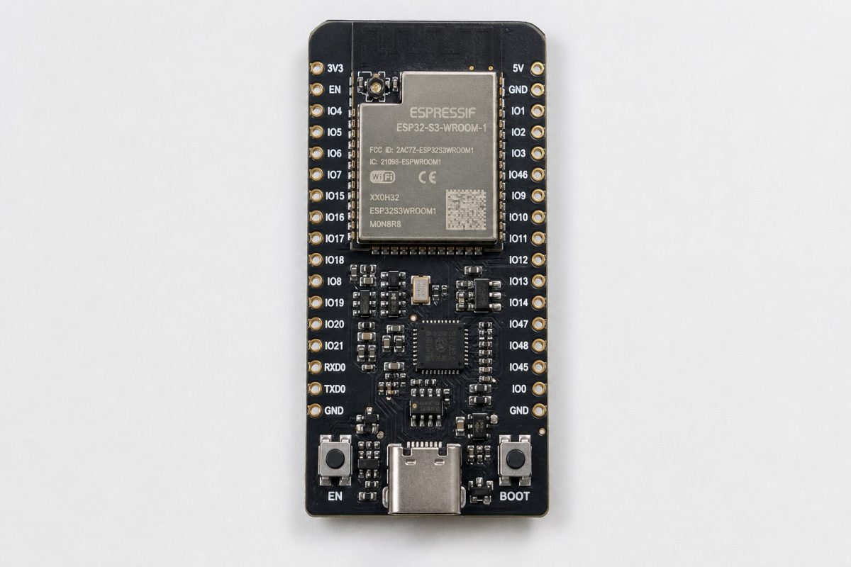
Pin names on the DevKit (J3 right header)
Right header J3, top to bottom:
1. G - Ground
2. TX - GPIO43, U0TXD (USB-serial TX to the PC)
3. RX - GPIO44, U0RXD (USB-serial RX)
4. 1 - GPIO1, TOUCH1, ADC1_CH0
5. 2 - GPIO2, TOUCH2, ADC1_CH1
6. 42 - GPIO42, JTAG MTMS
7. 41 - GPIO41, JTAG MTDI
8. 40 - GPIO40, JTAG MTDO
9. 39 - GPIO39, JTAG MTCK
10. 38 - GPIO38 (onboard RGB LED on v1.1)
11. 37 - GPIO37 (often taken by octal PSRAM / flash)
12. 36 - GPIO36 (same: leave free on N8R8 / N16R8 modules)
13. 35 - GPIO35 (same)
14. 0 - GPIO0 (boot / download strapping)
15. 45 - GPIO45 (strapping)
16. 48 - GPIO48 (RGB LED on some older DevKit revisions)
17. 47 - GPIO47
18. 21 - GPIO21 (common I2C SDA pick)
19. 20 - GPIO20, USB_D+
20. 19 - GPIO19, USB_D-
21. G - Ground
22. G - Ground
How to use the pin groups
Digital I/O. Most numbered pins are GPIO. Start with 1, 2, 4, 5, 6, 7, 8, 9, 10, 11, 12, 13, 14, 21, 47, 48.
Analog. ADC1 is safer while Wi-Fi is on: GPIO1, 2, 3, 4, 5, 6, 7, 8, 9, 10. ADC2 can fight Wi-Fi.
Touch. TOUCH1-14 map to GPIO1-14 (plus 3, 8, 9...). Use a short pad, not a long jumper.
UART. TX/RX (43/44) are the USB-serial link. UART1 is often GPIO17 (TX) and GPIO18 (RX).
I2C. Any free GPIO works in software. A common pair is GPIO8 (SDA) and GPIO9 (SCL), or GPIO21 plus a clock pin.
SPI. The FSPI pins on 9-14 are the easy hardware SPI set for displays and SD modules.
USB device. GPIO19 (D-) and GPIO20 (D+) are the native USB pair. Leave them alone if you use USB gadgets or USB-JTAG.
Do not use at boot or on many modules: GPIO0, 3, 45, 46, and 35-37 on octal PSRAM parts. Do not hang heavy loads on 3V3; drive motors from a separate 5 V / VIN supply and a driver board.
// ESP32-S3 DevKitC-1 v1.1 — blink the onboard RGB pin
// v1.1 LED is GPIO38. Some older boards use GPIO48.

#define LED_PIN 38

void setup() {
  pinMode(LED_PIN, OUTPUT);
}

void loop() {
  digitalWrite(LED_PIN, HIGH);
  delay(300);
  digitalWrite(LED_PIN, LOW);
  delay(300);
}
Applications
1. Wi-Fi products: PisoWiFi nodes, kiosks, and phone-controlled appliances.
2. BLE gadgets: beacons, HID keyboards, and phone pairing without a cloud.
3. USB gadgets: a native USB serial, MIDI, or storage device (GPIO19/20).
4. Cameras and vision: OV2640 / OV5640 boards, QR readers, simple inspection.
5. Local HMI: SPI TFT or OLED, touch buttons, RGB status.
6. Sensor islands: I2C temp/RH, air quality, current sense, then MQTT or a local API.
7. Audio: I2S mics and speakers for voice prompts or keyword detect.
8. Motor and LED control: PWM plus a driver; keep the power path off the 3V3 pin.
9. Edge AI demos: wake-word or tiny models in PSRAM.
10. Teaching firmware and turning a breadboard into a custom PCB.
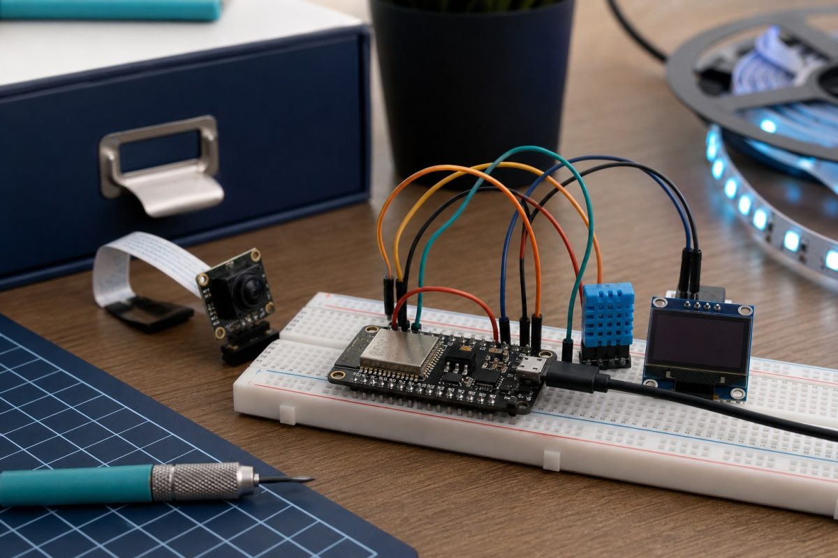
Sample projects to work on
1. First boot and RGB blink. Confirm COM port, USB driver, and GPIO38 vs GPIO48. Shop an ESP32-S3 board and a USB-C cable.
2. Wi-Fi weather node. DHT22 or SHT31 on I2C (GPIO8/9), post to a page or MQTT. Shop sensors plus a 5 V supply.
3. OLED status badge. SSD1306 on I2C, show IP and heap. Good first display project.
4. SPI TFT dashboard. Use FSPI pins 10-13 for a 2.4 or 3.5 inch panel. Add a touch overlay later.
5. USB serial gadget. Native USB on 19/20 so the board shows up as a COM device without the UART bridge.
6. BLE remote. Phone app toggles a relay module. Keep the relay on a driver and a separate 5 V rail.
7. Camera doorbell. OV2640 on the camera connector / GPIO set, save a still to SD (FSPI) and push a notice over Wi-Fi.
8. Voice prompt box. I2S mic in, small speaker out, play a clip when a button on GPIO4 is pressed.
9. LED art. WS2812 strip on GPIO47, 5 V from a real supply, one GND star back to the DevKit.
10. Custom PCB. Once the breadboard works, request a CraftedTech PCB design and fabricate through a print partner.
Start with 1-3 if you are new. Add a camera or I2S only after 3V3 current and boot pins are under control.