Arduino ATmega 2560 – KiCad Symbol, PCB Footprint, and 3D STEP File
Arduino ATmega 2560 – KiCad Symbol, PCB Footprint, and 3D STEP File
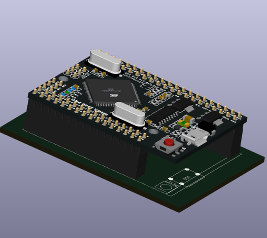
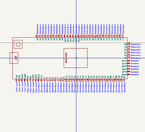
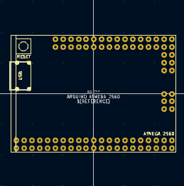
This package provides the KiCad symbol, PCB footprint, and 3D STEP model for the Arduino ATmega 2560 microcontroller board, one of the most powerful and versatile boards in the Arduino family. Featuring the ATmega2560 chip, this board offers 54 digital I/O pins, 16 analog inputs, 4 UARTs, and expanded memory, making it ideal for complex embedded systems, robotics, automation, and advanced electronics projects.
The KiCad symbol is designed for clean schematic integration, while the footprint ensures accurate PCB layout and compatibility with custom shield development. The included STEP file offers a precise 3D model that can be used for enclosure design, mechanical fitting, and visual renderings in tools such as Fusion 360, SolidWorks, and Altium.
This package is perfect for engineers, makers, and students who want to save time and improve accuracy when incorporating the Arduino Mega 2560 into their hardware designs.
Customize PCB
Customize PCB
 Need help building your PCB Message us on Facebook!
📩 INQUIRE with us on Messenger
PCB Layout & Design Services
We provide professional PCB layout and design services for electronics projects, prototypes, and small to medium production needs. Our goal is to deliver accurate, manufacturable, and well-documented PCB designs tailored to your specific requirements.
How to Request a PCB Layout/Design:
- Send your complete schematic or diagram via our Facebook page.
- We will assess your diagram and provide a quotation based on the complexity and requirements.
Special Offer for New Customers!!
New customers receive a special introductory discount on their first PCB layout/design project.
This allows us to review your design requirements and build a long-term working relationship.
How to Request a PCB Layout / Design
- Send your complete schematic or diagram via our Facebook page.
- Our team will review your diagram carefully to understand the design scope and requirements.
- A detailed quotation will be provided based on:
-
- Design complexity
- Board size and number of layers
- Components and package types
- Special routing or manufacturing requirements
📌 Providing your diagram is essential so we can give you an accurate and fair quotation.
PCB Layout & Design Requirements
To ensure quality and accuracy, please note the following:
- All schematics must be clear, complete, and properly labeled
- Specify:
- Board dimensions (if available)
- Number of PCB layers
- Preferred components or footprints (if any)
- Hand-drawn, unclear, or incomplete schematics are not accepted
- Rush or urgent requests may incur additional charges
What’s Included in the Design Package
Each completed project includes the following deliverables:
✅ 2D PCB layout images
✅ 3D PCB render images
✅ PCB Gerber files (ready for fabrication)
✅ Bill of Materials (BOM)
✅ Component Placement List (CPL / Pick-and-Place file)
✅ Wiring diagram (PDF)
✅ PCB board layout (PDF)
All files are prepared to be manufacturer-ready and easy to review.
Pricing Information
Pricing is project-based and depends on:
- The submitted schematic or diagram
- Board size and layer count
- Types of components used (SMD, through-hole, fine-pitch, BGA, etc.)
- Design complexity and routing difficulty
📌 Final pricing is confirmed only after reviewing the client’s diagram.
Design Review & Approval Process
Before final delivery:
- The client will receive preview files for checking
- Please review carefully for:
- Errors
- Missing information
- Clarifications or revisions
- Once the design is confirmed and approved, the final files will be sent to the client’s email
⚠️ After final approval, any major changes may be treated as a new request.
Payment Methods
Philippines (Local Clients):
- GCash
- Bank Transfer
International Clients:
- PayPal
📌 Design work starts after payment confirmation unless otherwise agreed.
SHOP Now and Enjoy Discount

![]()
Learn With CraftedTech Engineering
Learn With CraftedTech Engineering

Welcome to Learn With CraftedTech Engineering – your go-to hub for mastering the fundamentals and innovations in engineering and technology. Whether you're a student, hobbyist, or professional, our tutorials, project guides, and hands-on resources are crafted to empower your learning journey.
From Arduino and automation systems to PCB design, 3D models, and real-world engineering applications, we break down complex topics into easy-to-understand lessons. Explore, build, and innovate with us — because at CraftedTech Engineering, we don’t just teach; we craft your future innovations.